Fourier Surfaces
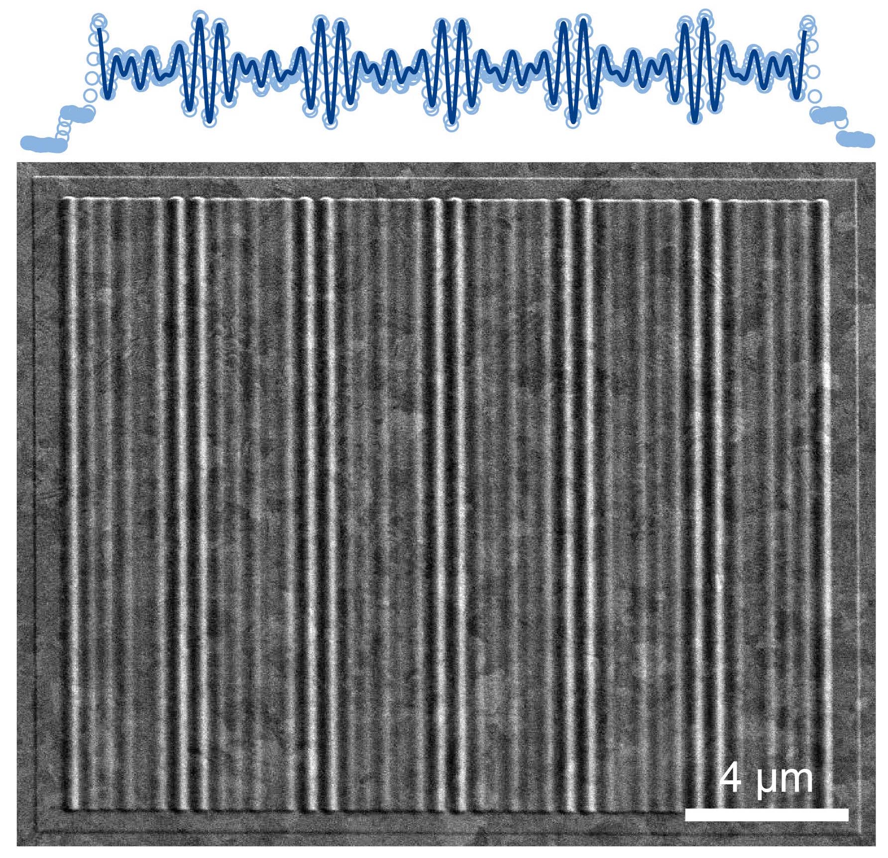
Modern communication relies on optical signals sent over optical fibers. To route and manipulate these signals, inexpensive, miniaturized and low-power photonic devices are required. Over the past decades, companies have leveraged the fabrication capabilities of the microelectronics industry to produce silicon chips that can perform these tasks, creating photonic integrated circuits. However, this technology also faces hurdles for further improvement. For example, the optical signal from the fiber must be transferred efficiently to/from the photonic chip. This operation is often done with a grating—a series of grooves that exploit diffraction to collectively redirect the light to/from a photonic “wire” (or waveguide) on the chip. Due to fabrication limitations, the groove shape, which plays a critical role in the performance of this transfer, is typically restricted to “square” cross sections. Unfortunately, Fourier optics teaches us that the ideal shape of the grating should be “wavy.” Because such wavy surfaces have not been possible to fabricate, straightforward solutions for specific photonic circuit elements have not been possible.
Recently, researchers in OMEL have resolved this issue (see figure above). Their technology1 provides a simple, powerful, and general route to arbitrary wavy surfaces. The resulting structures offer improved performance and new functionalities for many areas of optics. Researchers in OMEL are exploring the implications of this new method for applications in both optical and electronic devices.
- Lassaline, Brechbühler, Vonk, Ridderbeek, Spieser, Bisig, le Feber, Rabouw, & Norris. Optical Fourier Surfaces. Nature 582, 506 (2020). (external pageLink)